- My Portal
- Search
- Advise & Solutions
- Industries
- Calendar
- Solicitations
- Research
- tab 9
- tab 10
- tab 11
- tab 12
- tab 13
- tab 14
- tab 15
- tab 16
- tab 17
- tab 18
- tab 19
- tab 20
Catalog & Support
-
Instrumentation & Services
Find Products, Service Centers, Dealerships, Manuals, and more.
-
Business Services
Companies & Community
Support
Resources
_________________________ This section requires a Corporate membership _________________________
Products & Services Wanted
Featured Product
Electronics & Materials & Photonics
Hamamatsu
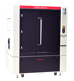
PHEMOS-X C15765-01
Semiconductor Failure Analysis System
- Description
- Specifications
- Reviews
- Offered by
- Availability
- tab 6
- tab 7
- tab 8
- tab 9
- tab 10
- tab 11
- tab 12
- tab 13
- tab 14
- tab 15
- tab 16
- tab 17
- tab 18
- tab 19
- tab 20
The PHEMOS-X is a semiconductor failure analysis system that can be equipped with up to five lasers having different output wavelengths from visible to near-infrared light. With just a single unit, the PHEMOS can localize failures with high sensitivity and high resolution. When a voltage is applied to a semiconductor device, the failure points in the semiconductor device emit light and heat. Scanning a semiconductor device with a laser beam while a voltage is applied to it causes the electrical current and operating state at the failure location to change. By utilizing these properties, the failure location can be estimated by detecting signals that represent changes in the semiconductor device caused by the applied voltage, laser scanning and visualizing those signals as images. At Hamamatsu Photonics we develop, manufacture and sell semiconductor failure analysis systems for various semiconductor devices in order to meet customer demands that vary with the constant advances made in semiconductor devices.
- Target device: Wafer (dicing chips, cracked wafers) Packaged IC (decapped IC, polished silicon substrate IC)
- Optical system movement range: Minimum resolution X axis: 0.05 μm, Y axis: 0.05 μm, Z axis: 0.05 μm Maximum movable range X axis: 40 mm, Y axis: 40 mm, Z axis: 80 mm Repeated positioning accuracy X axis: ±1.0 μm, Y axis: ±1.0 μm, Z axis: ±1.0 μm
- Camera: 2 cameras are selectable from CCD (400 nm to 1050 nm), InGaAs (900 nm to 1550 nm) and InSb (1500 nm to 5400 nm)
- Probing: Camera observation (Image is displayed on the touch screen.)
- Laser scan system: Spectral response range: 532 nm to 1340 nm, Mounts up to 5 light sources
- Lens: Macro lens port: 1, motorized revolver: 5 positions, optical magnification: 1.35x to 250x
- Software: Image acquisition and analysis software (SemiShop 4)
- Utility: Power: Single phase 200 V AC ± 20 V Power consumption: Approx. 3000 VA Vacuum source: 80 kPa or more Compressed air: 0.6 MPa to 0.7 MPa Dimensions: 1600 mm (W) ×1247 mm (D) × 2000 mm (H) Weight: Approx. 1800 kg
— no reviews —
Listings
New
0
0
0
Used
0
0
0
Rent-lease
0
0
0
Auction
0
0
0
Trade-Ins
0
0
0
Donations
0
0
0
Authorized Dealers
0
0
0
All Registered Trademarks, brand names and logos are respected and their ownership acknowledged. They are used on this website for information and reference purposes only. Test Interest doesn't assume any other implication or representation.
TI-1-3